Peneira molecular de carbono na indústria de semicondutores: material essencial para o fornecimento de nitrogênio de ultra-alta pureza.
Jul 10, 2026
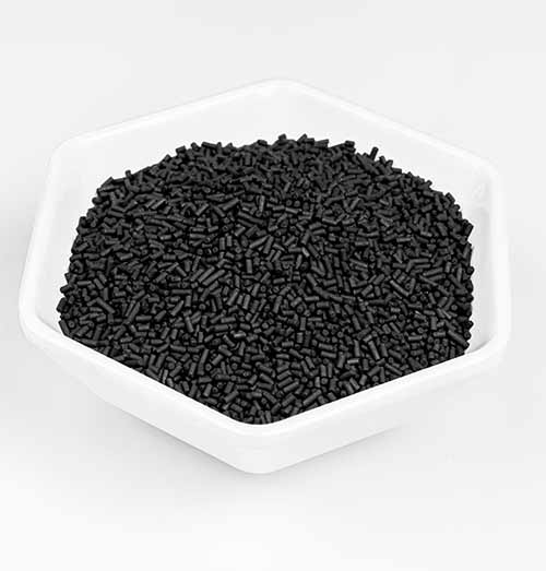
A fabricação de componentes eletrônicos e semicondutores impõe padrões extremamente rigorosos de limpeza ambiental e atmosfera livre de oxigênio e umidade. Traços de oxigênio, vapor d'água e impurezas podem causar oxidação do wafer, defeitos nos circuitos e falhas nos chips, reduzindo drasticamente o rendimento do produto. É necessário um fornecimento massivo e ininterrupto de nitrogênio de altíssima pureza como gás de proteção, gás de purga e gás de arraste em todos os processos de produção. A geração de nitrogênio por PSA no local tornou-se a principal solução de fornecimento de gás para fábricas de wafers e plantas de embalagem. A peneira molecular de carbono (CMS) serve como adsorvente principal para a separação precisa de nitrogênio e oxigênio. Combinada com unidades de pós-purificação, ela garante o fornecimento estável de nitrogênio de ultra-alta pureza (6N) para semicondutores avançados. Este artigo detalha as funções exclusivas, os cenários de aplicação, as vantagens exclusivas do setor e os critérios de seleção dos sistemas de gerenciamento de configuração (CMS) adaptados às demandas da fabricação de semicondutores. 1. Por que o nitrogênio de ultra-alta pureza é essencial para a produção de semicondutores? Traços de oxigênio e umidade no ar causam danos irreversíveis aos processos de fabricação de semicondutores de precisão:Oxidação de wafers de silício, circuitos de cobre e alumínio, causando fuga de corrente e curto-circuitos.Exposição prematura do fotorresiste, largura de linha distorcida e rugosidade da borda da linha durante a litografia.Contaminantes residuais de flúor dentro das câmaras de gravação a plasma causam defeitos na superfície do wafer.A corrosão dos equipamentos de feixe de íons e o ozônio geram partículas de óxido metálico que causam arranhões na superfície do wafer.Oxidação, juntas de solda frias e baixa confiabilidade de componentes eletrônicos durante a soldagem SMT. O nitrogênio é quimicamente inerte e seco, isolando o ar e criando um ambiente de produção livre de contaminação. Processos avançados de semicondutores exigem pureza de nitrogênio acima de 99,999% (5N ou superior). Materiais comuns de separação de gases não conseguem manter essa alta pureza de forma estável; o CMS especial de alta qualidade é o adsorvente ideal para atender a esses rigorosos requisitos de pureza em sistemas de nitrogênio PSA in loco. 2. Principais cenários de aplicação do nitrogênio PSA da CMS na cadeia industrial de semicondutores 2.1 Fabricação de wafers front-endLitografia (EUV/DUV): Estágios de purga do wafer e câmaras de vácuo para bloquear o oxigênio e evitar a exposição prematura do fotorresiste, garantindo precisão nanométrica na largura da linha.Gravação a seco e remoção de resíduos por plasma: Substituição da câmara e purga com fluoreto residual para evitar a oxidação da parede lateral do wafer de silício.Deposição de Filmes Finos por CVD e PVD: Gás de arraste e gás de proteção do forno para isolar o ar e prevenir a oxidação das camadas de cobre/alumínio sob alta temperatura.Implantação iônica: Resfriar os dutos do feixe de íons, suprimir a formação de ozônio e proteger os wafers e os componentes da câmara contra corrosão.Recozimento térmico rápido: atmosfera de nitrogênio seco para eliminar a oxidação do substrato de silício e estabilizar a uniformidade da dopagem. 2.2 Embalagem e TestesCorte do wafer, montagem do chip e moldagem sob atmosfera inerte de nitrogênio para evitar a oxidação do chip exposto.Proteção com nitrogênio para soldagem por refluxo e onda, visando reduzir a oxidação da junta de solda, a formação de vazios e a soldagem fria.Câmaras de teste de envelhecimento preenchidas com nitrogênio para isolar a umidade e o oxigênio, garantindo testes de desempenho elétrico estáveis. 2.3 Cenários de Instalações AuxiliaresPurga de dutos e equipamentos antes da manutenção para eliminar riscos residuais de gases especiais inflamáveis.Cobertura com nitrogênio para tanques de armazenamento de produtos químicos e fotorresistentes para prevenir a deterioração oxidativa.Purga a seco para salas limpas e câmaras de processo, visando manter um ponto de orvalho baixo e padrões de ausência de poeira. 3. Vantagens exclusivas do nitrogênio PSA da CMS para cenários de semicondutores 3.1 Saída estável de ultra-alta purezaO CMS de grau semicondutor, com controle de poros de precisão sub-angstrom, proporciona seletividade excepcional na separação de oxigênio. A flutuação da pureza do nitrogênio permanece mínima durante a operação de longo prazo, atendendo consistentemente aos padrões 5N/6N para processos avançados e reduzindo as taxas de refugo de wafers. 3.2 Desempenho estável em ciclos longos para produção ininterruptaO material tolera traços de vapores ácidos e alcalinos e suporta altas temperaturas dentro dos limites de projeto, mantendo ciclos estáveis de adsorção-dessorção mesmo com traços de impurezas corrosivas no ar comprimido. Sua vida útil atinge de 8 a 10 anos com fornecimento de ar comprimido limpo e bem filtrado, minimizando as perdas por paradas de produção causadas pela substituição frequente do material. 3.3 Baixa geração de poeira para atender aos padrões de salas limpasA elevada resistência mecânica e a formulação com baixa geração de poeira evitam a liberação de partículas finas de carbono durante a adsorção, prevenindo a contaminação por partículas em wafers e equipamentos de precisão, de forma a atender às especificações de salas limpas Classe 100/1000 (ISO 5/ISO 6). 3.4 Operação com economia de energia e baixa emissão de carbonoA adsorção por oscilação de pressão à temperatura ambiente consome muito menos energia do que a separação criogênica. O baixo consumo de energia por metro cúbico de nitrogênio reduz os gastos com eletricidade em grandes fábricas de wafers e apoia a fabricação eletrônica de baixo carbono. 4. Como a qualidade do CMS impacta o rendimento e os custos operacionais dos semicondutores Os processos de fabricação de semicondutores têm uma tolerância extremamente baixa a impurezas gasosas. O desempenho do CMS (Sistema de Gerenciamento de Carga Química) determina diretamente o rendimento dos chips e os custos de manutenção dos equipamentos. 4.1 Desempenho superior de CMS de alta qualidade para semicondutoresEficiência de separação de oxigênio e nitrogênio ultra-alta com baixo consumo de ar para reduzir os custos de energia do compressor de ar.Pureza de nitrogênio ultra-alta sustentada de 5N a 6N sem efeito rebote de oxigênio durante longos ciclos de operação.Alta resistência à compressão das partículas e propriedades antipulverização para evitar contaminação por poeira em processos limpos.Resistência a manchas de óleo e traços de impurezas ácidas/alcalinas para adaptação a fontes de ar pré-filtradas de fábrica.A alta velocidade de regeneração permite o fornecimento ininterrupto de nitrogênio por meio da comutação da torre, adequando-se à produção contínua de grande volume. 4.2 Perdas de Produção Causadas por um CMS InferiorA pureza inadequada do nitrogênio, com excesso de oxigênio, leva à oxidação em massa dos wafers e à queda acentuada do rendimento.O consumo elevado de ar força os compressores a funcionarem em plena carga, aumentando as contas de eletricidade a longo prazo.A pulverização gera poeira de carbono que bloqueia tubulações e contamina wafers, aumentando a frequência de limpeza dos equipamentos.A rápida deterioração do desempenho exige frequentes paradas na produção para a substituição do CMS (Sistema de Gerenciamento de Chips), interrompendo a fabricação de chips 24 horas por dia, 7 dias por semana. 5. Padrões de seleção de CMS adaptados para a indústria eletrônica e de semicondutores As fábricas de semicondutores e as unidades de embalagem devem concentrar-se em indicadores específicos do setor durante a aquisição de sistemas de gerenciamento de componentes (CMS):Padrão de pureza de nitrogênio exigido por diferentes processos (5N para embalagens / 6N para litografia avançada)Fluxo contínuo de nitrogênio de grande volume, 24 horas por dia, que atenda à demanda total de gás da fábrica.Resistente à poeira e com alta resistência mecânica para atender aos requisitos de descontaminação de salas limpas.Vida útil e estabilidade da pureza sob operação prolongada com oscilação cíclica de pressão.Baixo teor de cinzas e baixa lixiviação de metais pesados para atender às especificações de ausência de poeira e metais pesados em semicondutores.Compatibilidade com geradores de nitrogênio PSA industriais de grande vazão. Fornecedores profissionais de CMS podem personalizar adsorventes para chips lógicos, chips de memória, embalagens avançadas e fabricação de painéis, equilibrando a eficiência da produção de nitrogênio, a pureza e os custos operacionais abrangentes a longo prazo. 6. ConclusãoO nitrogênio de ultra-alta pureza serve como gás de processo fundamental para a fabricação, embalagem e teste de wafers na indústria de semicondutores. Como principal material funcional dos geradores de nitrogênio PSA instalados no local, a CMS possibilita o fornecimento de nitrogênio de ultra-alta pureza de forma estável, contínua e a baixo custo. O sistema CMS premium específico para semicondutores não só fornece nitrogênio de forma constante em concentrações de 5N a 6N para eliminar defeitos de processo induzidos por oxigênio e umidade e aumentar o rendimento dos chips, como também apresenta baixo consumo de energia, baixa emissão de poeira e longa vida útil, reduzindo os gastos gerais da fábrica com fornecimento de gás e manutenção de equipamentos. Seja para litografia avançada, deposição de filmes finos e implantação iônica em processos front-end, ou para soldagem SMT e encapsulamento de chips em estágios back-end, selecionar um CMS de alto desempenho adequado às condições de trabalho é um investimento crítico para empresas de eletrônicos e semicondutores, a fim de garantir a qualidade do produto e viabilizar uma produção em massa estável.


 SUPORTADO POR REDE